Supercon 6 (2022) · Volume 1
Voja4 (Supercon 6, 2022) Volume 1 — Architecture
The 4-bit CPU, the 12-bit instruction word, every register and SFR, the full 31-instruction ISA cheat sheet, and the modes
Introduction
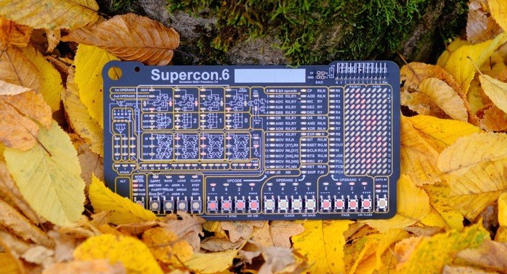
The 2022 Hackaday Superconference 6 badge — designed by Voja Antonic and known internally as the Voja4 — is a hypothetical 4-bit CPU simulated in firmware on a Microchip PIC24FJ256GA704-I/PT host microcontroller. The point is education: you program it directly in machine code by punching binary instructions into front-panel buttons, watching a 16×17 LED matrix show every register, flag, and decoded opcode in real time. It’s an Altair-8800-spirit teaching machine, but where every internal node of the CPU is visible — the operand registers, the adder inputs, intermediate carries, accumulator master-slave flip-flops, the carry-input inverter for subtraction, and the bit-by-bit data path. That visibility is the design.
This volume covers the architecture as captured in the five official manuals shipped in the upstream repo (manuals/). The deeper “why” choices (e.g. why master-slave flip-flops are drawn out instead of hidden, why PCL/PCM/PCH are exposed as writable registers) are touched on briefly; for full firmware/toolchain detail see vol2 (firmware) and vol3 (Python assembler + emulator).
📷 Hero photo:
03-outputs/figs/voja4_hero.jpg
1.1 CPU overview
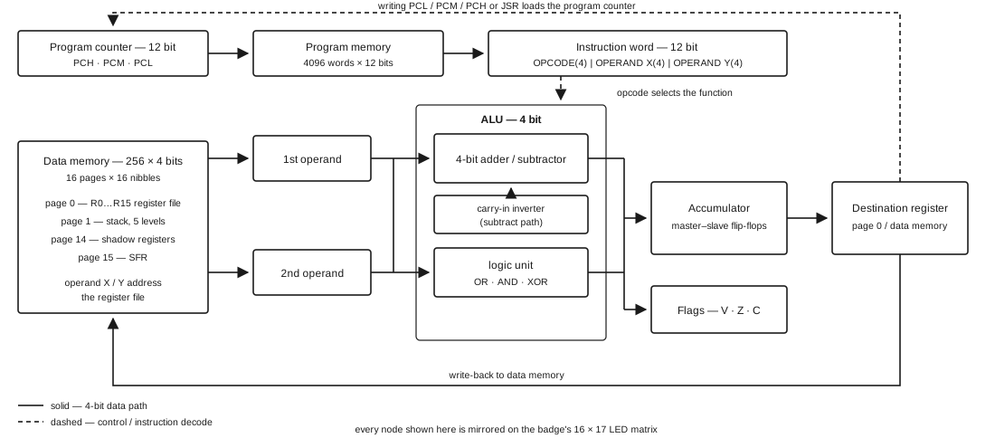
Datapath: 4-bit. The visible “processor” is a single accumulator architecture with a 4-bit ALU (adder/subtractor + OR/AND/XOR logic gates).
Instruction word: 12 bits, fixed length. Encoded as one of:
OPCODE(4) | OPERAND_X(4) | OPERAND_Y(4)— when opcode is 4 bits0000 | OPCODE(4) | OPERAND_Y(4)— when opcode is 8 bits and there’s one operand0000 | OPCODE(4) | RG(2) | M(2)— forBIT/BSET/BCLR/BTG(operand Y split 2+2)
So there are at most 15 four-bit-opcode instructions (opcode 0001–1111) and 16 eight-bit-opcode instructions (0000_0000–0000_1111). Total instructions in the released ISA: 31.
Program memory: 4096 words × 12 bits (4K words). Program Counter is 12 bits.
Data memory: 256 nibbles × 4 bits, organized as 16 pages of 16 nibbles each.
Clock: user-selectable in 15 discrete steps from 0.5 Hz to 100 kHz, plus a 16th “max” step at roughly 250 kHz. Every instruction takes one clock cycle, so peak throughput is ~0.25 MIPS. The slowest step (0.5 Hz, one instruction every 2 seconds) is the headline feature — it’s the speed at which you can watch the data path advance.
Host MCU: PIC24FJ256GA704 (16-bit, 256 KB Flash). The 4-bit CPU is a software simulation; the PIC also drives the LED matrix multiplex, scans the button matrix, runs the UART, manages the bootloader, etc. See Hardware manual §1 for the schematic; the only other ICs of note are two 74HC138 3-to-8 decoders that drive the LED matrix cathodes.
Power: 2 × AA alkaline (3 V nominal). 5.5 µA in sleep; ~27 mA running with 40 LEDs on (typical). Full battery life on fresh AAs is ~3 days of continuous operation; works down to 1.82 V (just dim). Auto-off triggers after 20 minutes from boot or 2.5 hours of no keypress.
1.2 Register file and data memory map
The simulated CPU’s register file is a section of data memory — there is no separate register file. Page 0 (data memory addresses 0x00–0x0F) holds the 16 main registers:
Table 1 — The simulated CPU's register file is a section of data memory — there is no separate register file. Page 0 (data memory addresses 0x00–0x0F) holds the 16 main registers
| Addr | Name | Purpose |
|---|---|---|
| 0x00 | R0 | General purpose. Also the destination of RET R0,N (lookup-table convention). |
| 0x01–0x09 | R1–R9 | General purpose. |
| 0x0A | OUT (R10) | Output port (4 bits). Can be remapped to SFR page (see WrFlags.IOPos). |
| 0x0B | IN (R11) | Input port (4 bits). Can be remapped to SFR page. |
| 0x0C | JSR | Writing here triggers a subroutine call. PCM/PCH must be pre-loaded. |
| 0x0D | PCL | Writing here triggers a long jump. PCM/PCH must be pre-loaded. |
| 0x0E | PCM | Mid nibble of jump/call target (bits 7–4 of the 12-bit address). |
| 0x0F | PCH | High nibble of jump/call target (bits 11–8). |
Only
MOV RX,RY/MOV RX,N/INC RY/DEC RYinstructions trigger the jump/call behavior when their destination isPCLorJSR. Bit-set/clear instructions targeting those addresses do not trigger it. (User Manual §“Programmer’s model”.)
Page 1 (0x10–0x1F) is the stack. Stack Pointer is a 3-bit register, not directly visible to user code; calls push the 12-bit PC (3 nibbles) at 0x10 + 3×SP then increment SP. Maximum 5 levels of nesting (15 nibbles used; 0x1F is unused and available as general-purpose RAM). The 6th call or a return underflow is a fatal error — execution halts with the stack indicator blinking the offending value (110 for overflow, 111 for underflow).
Pages 2–13 (0x20–0xDF): general-purpose RAM (192 nibbles, 96 bytes).
Page 14 (0xE0–0xEF): shadow register area. The EXR N instruction atomically swaps the first N registers of Page 0 with the first N nibbles of Page 14 — a fast register-bank switch, useful for interrupt-like context save. A panel LED toggles every EXR so you can see whether you’re “swapped” or “restored.”
Page 15 (0xF0–0xFF): Special Function Registers (SFR):
Table 2 — Page 15** (`0xF0`–`0xFF`): **Special Function Registers (SFR)
| Addr | Name | Purpose |
|---|---|---|
| 0xF0 | Page | 4-bit register that selects which page is shown on the right half of the LED matrix (left half is Page+1, wrapping). |
| 0xF1 | Speed | Processor clock selector (0–15, see clock table in Instruction Set manual). |
| 0xF2 | Sync | Heartbeat / sync timer selector (0–15, periods 1 ms to 1 s). |
| 0xF3 | WrFlags | Control bits: RxTxPos (UART pin routing), IOPos (IN/OUT remap), MatrixOff, LedsOff. |
| 0xF4 | RdFlags | Status: UserSync bit 0, V flag bit 1, and others (read-only). |
| 0xF5 | SerCtrl | Baud rate selector for general UART (does NOT affect SAVE/LOAD which is fixed at 9600). |
| 0xF6–0xF7 | SerLow/SerHigh | Serial TX byte (write to send). |
| 0xF8 | Received | Serial RX byte (read after RxReady). |
| 0xF9 | AutoOff | Auto-shutoff countdown, 10-min resolution; write 15 = 2.5 h, write 0 = off now. |
| 0xFA | OutB | Mirror of OUT when remapped (WrFlags.IOPos=1). |
| 0xFB | InB | Mirror of IN when remapped. |
| 0xFC | KeyStatus | Button state. |
| 0xFD | KeyReg | Last key code. |
| 0xFE | Dimmer | LED PWM duty cycle (6%–100%). |
| 0xFF | Random | Pseudorandom number generator. |
Flag access subtlety: the V (Overflow) flag is not in a SKIP condition — to test it, read
RdFlags.bit1withBIT RdFlags, 1. Z and C are direct SKIP conditions.
1.3 Instruction set
The 31 instructions fall into seven groups. The full per-instruction reference (with cycle-by-cycle behavior, flags affected, examples) is in manuals/2.Instruction_Set_v4.pdf — this section is a quick-reference cheat sheet for writing programs.
4-bit-opcode instructions (opcode 0001–1111):
Table 3 — 4-bit-opcode instructions (opcode 0001–1111)
| Opcode | Mnemonic | Description | Flags affected |
|---|---|---|---|
| 0001 | ADD RX, RY | RX ← RX + RY | V, Z, C |
| 0010 | ADC RX, RY | RX ← RX + RY + C | V, Z, C |
| 0011 | SUB RX, RY | RX ← RX − RY | V, Z, C |
| 0100 | SBB RX, RY | RX ← RX − RY − ~C | V, Z, C |
| 0101 | OR RX, RY | RX ← RX | RY | Z |
| 0110 | AND RX, RY | RX ← RX & RY | Z |
| 0111 | XOR RX, RY | RX ← RX ^ RY | Z |
| 1000 | MOV RX, RY | RX ← RY (writing PCL/JSR triggers jump/call) | — |
| 1001 | MOV RX, N | RX ← literal nibble N (writing PCL/JSR = jump/call) | — |
| 1010 | MOV [XY], R0 | Data memory[XY] ← R0; XY is a register pair address | — |
| 1011 | MOV R0, [XY] | R0 ← Data memory[XY] | — |
| 1100 | MOV [NN], R0 | Data memory[NN] ← R0; NN is the full 8-bit operand as an immediate address | — |
| 1101 | MOV R0, [NN] | R0 ← Data memory[NN] | — |
| 1110 | MOV PC, NN | Long jump within current page (PC ← {PCH:PCM:NN}) — actually loads PC low 8 bits from NN | — |
| 1111 | JR NN | Relative jump: PC ← PC + signed(NN). Note: PC has already been auto-incremented, so JR -1 (1111 1111 1111) is the dead-loop pattern. | — |
8-bit-opcode instructions (opcode 0000, sub-opcode in operand X bits 7–4):
Table 4 — 8-bit-opcode instructions (opcode 0000, sub-opcode in operand X bits 7–4)
| Sub-op | Mnemonic | Description | Flags |
|---|---|---|---|
| 0001 | CP R0, N | R0 − N (result discarded, flags set). | V, Z, C |
| 0010 | ADD R0, N | R0 ← R0 + N | V, Z, C |
| 0011 | INC RY | RY ← RY + 1 (writing PCL/JSR triggers jump/call — used for “next entry” lookup tables) | V, Z, C |
| 0100 | DEC RY | RY ← RY − 1 | V, Z, C |
| 0101 | DSZ RY | DEC RY, then skip next instruction if zero. The badge’s primary loop primitive. | — |
| 0110 | OR R0, N | R0 ← R0 | N. With N=1 at addr Carry = set carry; with N=0xF = set all. | Z |
| 0111 | AND R0, N | R0 ← R0 & N. With N=0 = clear R0/carry. | Z |
| 1000 | XOR R0, N | R0 ← R0 ^ N. With N=0xF = complement R0; with carry = toggle carry. | Z |
| 1001 | EXR N | Swap first N+1 registers of Page 0 ↔ Page 14 (shadow swap). | — |
| 1010 | BIT RG, M | Test bit M of register RG; load !bit into Z. RG and M are 2-bit fields. | Z |
| 1011 | BSET RG, M | Set bit M of RG. | — |
| 1100 | BCLR RG, M | Clear bit M of RG. | — |
| 1101 | BTG RG, M | Toggle bit M of RG. | — |
| 1110 | RRC RY | Rotate RY right through carry. | C, Z |
| 1111 | RET R0, N | SP—, PC ← stack, R0 ← N (the N supports lookup-table call/return pattern). | — |
| (special) | SKIP F, M | Skip next instruction if flag F (Z or C) equals M. Encoded with the BIT-family operand split. | — |
Bit-instruction RG field encoding (2 bits — addresses one of four registers): the Bit Test/Set/Clear/Toggle and SKIP instructions can only operate on a limited set of registers because they encode the register in just 2 bits. See the instruction-set manual for the exact mapping; in practice R0, R1, R2, R3 are the common targets.
1.3.1 Synthetic (“pseudo”) instructions
The Voja4 ISA has gaps that the manual fills with macros — these aren’t separate opcodes, just useful sequences:
Table 5 — The Voja4 ISA has gaps that the manual fills with macros — these aren't separate opcodes, just useful sequences
| Pseudo | Implementation | Notes |
|---|---|---|
RLC RX, RY (rotate left through carry) | MOV RX, RY + ADDC RX, RY | Result in RX |
SL RX, RY (shift left) | MOV RX, RY + ADD RX, RY | Result in RX |
LSR RY (logical shift right) | AND R0, 0 + RRC RY | Clears carry first |
CPL R0 (complement) | XOR R0, 0xF | |
CPL RX, RY | MOV RX, 0xF + SUB RX, RY | |
NEG RX, RY (negate) | MOV RX, 0 + SUB RX, RY | |
NOP | MOV R0, R0 (any reg except R12/R13) | R12=JSR / R13=PCL would trigger a jump/call! |
1.3.2 Programmer’s pitfalls (worth tattooing on the inside of your eyelids)
NOPisMOV R0, R0, NOTMOV PCL, PCL— writing to PCL initiates a jump.JR -1for a dead loop — notJR 0. PC is auto-incremented before the relative add.JR -1encodes as1111 1111 1111.- Multi-nibble arithmetic uses Little-Endian convention in the example code: process LSB first with ADD/SUB, then propagate with ADC/SBB. Example for two 16-bit (4-nibble) numbers in R0–R3 + R4–R7:
ADD R0,R4 / ADC R1,R5 / ADC R2,R6 / ADC R3,R7. - V flag has no SKIP condition — test via
BIT RdFlags, 1. - A subroutine call costs 4 stack writes (12-bit PC + 4-bit N latency) and SP only goes to 5. Recursion is out.
- Long jumps require pre-loading PCM and PCH (then writing PCL kicks it off). Within a single 256-word page you can use
MOV PC, NNfor an 8-bit immediate. RET R0, Nloads the literal N into R0 as part of the return. This is the canonical pattern for lookup-table returns (subroutine indexes a table, returns the value via R0).
1.4 Addressing modes (brief)
- Register direct:
RX, RY— first nibble of data memory (page 0). - Immediate:
N(4-bit),NN(8-bit for jump targets / memory addresses). - Indirect via register pair:
[XY]— the operand X and Y values themselves form an 8-bit Data Memory address. SoMOV [XY], R0writes R0 to address formed by(RX << 4) | RY. RX is the page (0–15), RY is the offset within the page. - Direct memory:
[NN]— the 8-bit literal NN is the data memory address.
There is no register-indirect-with-displacement, no PC-relative data fetch, and no real indirect via memory.
1.5 Memory map summary
See §2 for the detail. At a glance:
DATA MEMORY (256 nibbles, 16 pages × 16):
  0x00–0x0F  Page  0   Main registers (R0–R9 + OUT/IN/JSR/PCL/PCM/PCH)
  0x10–0x1F  Page  1   Stack (5 levels = 15 nibbles; 0x1F free)
  0x20–0xDF  Page  2–13  General-purpose RAM
  0xE0–0xEF  Page 14   Shadow register area (swap with Page 0 via EXR)
  0xF0–0xFF  Page 15   Special Function Registers

PROGRAM MEMORY: 4096 words × 12 bits
HOST FLASH: 16 user-program slots saved to PIC Flash via DIR mode Save/Load.
1.6 IO peripherals
- LED matrix: 16×17, ~272 LEDs (182 red + 90 yellow per the Hardware manual). Anode-driven by PIC port pins, cathode-driven by two 74HC138 decoders. Multiplexed; the dimmer is duty-cycle PWM. Two SFR bits (
WrFlags.MatrixOff,WrFlags.LedsOff) let user code turn parts of the display off — note that the CLK indicator can NEVER be disabled, so you always know the unit is running. - Buttons: ~20 buttons total (18 in the main matrix + ALT + ON-OFF), scanned through the same matrix.
- UART: 1200–115200 baud (default 2400; SerCtrl-selectable); 3 V CMOS. Routed to either the I/O connector (default) or to the SAO connector (WrFlags.RxTxPos=1). Tx is also always available on SAO. Program Save/Load is always 9600,N,8,1 on the I/O connector — not affected by SerCtrl.
- I/O connector: 4 inputs + 4 outputs (4-bit each), plus the 5 ICSP pins for re-flashing the host PIC. Inputs are the IN register (R11 or 0xFB), outputs are OUT (R10 or 0xFA). All inputs have 22 kΩ pull-ups, all outputs have 22 kΩ pull-downs (Tx is the exception with a pull-up).
- SAO (“Shitty Add-On”) connector: Power (GND, +3 V) + UART (Tx/Rx). NO I²C — non-standard for SAO.
- Internal Flash storage: 15 user program slots (slot 15 has a special function — it’s the auto-backup before a Load).
1.7 Modes
Table 6 — 7. Modes
| Mode | Acronym | Behavior |
|---|---|---|
| Direct | DIR | No program memory; instructions execute as you build them on the panel. Best for “what does ADC do to these inputs?” experimentation. Most instructions work; data-memory ones don’t. Also where SAVE/LOAD happen. |
| Single Step | SS | Step through Program Memory one instruction at a time via the STEP button. Includes a HISTORY submode that records the last 127 steps with all register/memory state — so you can walk backward through execution. |
| Run | RUN | Free execution at the configured clock speed. Includes PAUSE, BREAK, FAST (10× clock) controls. |
| Program | PGM | Editor for Program Memory. DEP+ writes the current panel state to the addressed word, ALT-DEP+ inserts (shift down), ALT-ADDR SET deletes (shift up). |
Two special boot-modes: TEST (LED + button hardware check, enter by holding ALT during reset) and BOOTLOAD (firmware re-flash via UART at 9600,N,8,1, enter by holding ALT+LOAD during reset).
1.8 Relation to prior Voja Antonic designs
The Voja4 is the fourth in a recognizable lineage of Voja Antonic computer designs spanning ~40 years. The through-line is “learn the machine by watching it operate at human speed” — every design exposes more internal state than is strictly necessary for users, because Voja’s audience is people who want to understand the architecture, not just operate the machine.
1.8.1 Galaksija (1983-1984)
Voja’s first widely-built design was the Galaksija — Yugoslavia’s first widely-used home computer and very nearly the country’s only one. Z80-based, 4 KB of ROM holding a custom BASIC interpreter shoehorned in (Microsoft BASIC wouldn’t fit), 2-6 KB of RAM, a 32×16 character video display generated by clever Z80-as-video-generator timing tricks (no dedicated video chip), and a 54-key membrane keyboard. The schematic, PCB layout, and full source listing were published in a 1983 issue of the Yugoslav magazine Računari u vašoj kući (“Computers in Your Home”) with kit-quality detail; readers built thousands. The Galaksija established Voja’s design signature: maximum capability per part, full transparency of internal operation, and a published-for-amateurs ethos. That signature carries through every later badge.
1.8.2 Hackaday Belgrade 2016 / Supercon 2016 — The first SuperCon badge
The first Hackaday SuperConference (Pasadena, November 2016) badge was based on a design Voja had developed for the Hackaday Conference in Belgrade (April 2016). It was an exposed-PCB device with:
- PIC18LF25K50 host MCU
- 8 × 16 surface-mount LED matrix (128 LEDs in a grid)
- 4 user buttons (plus reset and wake-from-sleep)
- IR communication (badge-to-badge interaction was a key design goal)
- Three-axis accelerometer
- Expansion connector for add-ons
This established the SuperCon badge formula Voja would refine: PIC microcontroller, a lot of visible LEDs in a fixed grid, minimal buttons, expansion contacts. The 2016 badge ran a small interactive demo firmware but was primarily a hacking platform — the hardware itself was the point, not a finished application.
1.8.3 Hackaday Belgrade 2018 / Supercon 2018 — The retro-computer badge
The 2018 Belgrade badge (then brought essentially unaltered to Supercon 2018 in November) was Voja’s first virtual-machine-on-a-badge design — a clear philosophical precursor to the Voja4. It was a stand-alone, battery-powered “vintage computer,” featuring:
- 320 × 240 pixel color LCD (a real display, not a LED grid)
- Full QWERTY keyboard built into the PCB
- Custom virtual CPU running on the host PIC (32-bit, not 4-bit — it was a more conventional retro-computer experience)
- BASIC interpreter + a CP/M emulator + a games suite, all in firmware
- Battery-powered, hand-held form factor
The 2018 badge prioritized doing things with the badge (you could write programs, play games, walk around comparing scores) — it was a complete retro-computer-in-your-hand. The Voja4 inverts this: doing little, teaching a lot.
1.8.4 Supercon 6 (2022) — The Voja4
After three years off (no in-person Supercon during COVID), the November 2022 badge — covered in this deep dive — represents the strongest distillation yet of the Galaksija ethos. Compared to its predecessors:
Table 7 — After three years off (no in-person Supercon during COVID), the November 2022 badge — covered in this deep dive — represents the strongest distillation yet of the Galaksija ethos. Compared to its predecessors
| Feature | 2016 Supercon | 2018 Belgrade / Supercon | Voja4 (2022) |
|---|---|---|---|
| Visible LEDs | 128 (matrix) | (display only) | 272 (incl. internal CPU state) |
| Buttons | 4 + reset | full QWERTY | ~20 (CPU-panel style) |
| Virtual CPU | — | 32-bit, BASIC-running | 4-bit, panel-programmed |
| Display | LED matrix | 320×240 color LCD | LED matrix |
| Stored programs | — | full filesystem | 15 PIC Flash slots |
| User clock control | — | — | 0.5 Hz – 250 kHz, 16 steps |
| ALU internals exposed | — | — | YES — adders, carries, ACC |
The Voja4 is the only one of the four where the host PIC’s role is to simulate a different, simpler CPU for educational purposes, with every internal node of that simulated CPU on a panel LED. The 2016 badge was hardware-as-platform. The 2018 badge was a retro-computer-as-product. The 2022 badge is a CPU-as-teaching-instrument — closer in spirit to a 1970s Altair 8800 front panel than to any home computer Voja built before.
1.8.5 Design through-lines (40 years of them)
- Maximum information density on the front face. Galaksija front-loaded the keyboard + display + every status LED into a single user-facing plane; the 2016/2022 SuperCon badges did the same with LED grids; even the 2018 badge surfaces every program/system state on its color display rather than hiding it behind menus.
- Published with build-it-yourself fidelity. Galaksija schematics in Računari with full part lists; SuperCon badges with complete design files, firmware sources where licensing allowed, and detailed manuals (the Voja4 ships five manuals in the upstream repo).
- PIC as the universal host. The 2016 badge used PIC18LF25K50; the 2022 Voja4 uses PIC24FJ256GA704. Voja’s vehicle of choice for “small reliable hand-held computing thing” has stayed within the Microchip 8-bit/16-bit PIC family for a decade.
- The instruction word is the user interface. The Galaksija manual taught Z80 assembly with the assumption you’d poke instructions in by hand; the Voja4 makes that literal — there is no keyboard, you build the instruction word on the front panel buttons.
Reading order: if you want the design lineage but aren’t building one of the older badges, the 2018 Belgrade badge’s project page on hackaday.io and the 2016 SuperCon badge teardown article on hackaday.com are the two most useful primary sources — both are linked from
02-inputs/research/links.md.
References
02-inputs/research/manuals/1.User_Manual_v4.pdf— modes, panel callouts, indicators02-inputs/research/manuals/2.Instruction_Set_v4.pdf— full ISA reference (the cheat sheet in §3 is sourced from here)02-inputs/research/manuals/3.Special_Function_Registers_v4a.pdf— SFR detail (§2 table above is a summary)02-inputs/research/manuals/4.DIR_Mode_v4.pdf— DIR-mode specifics02-inputs/research/manuals/5.Hardware_v4b.pdf— schematic, LED matrix wiring, power02-inputs/research/2022-Supercon6-Badge-Tools/firmware/—Badge_v99r3.bin(PIC24 binary; source not in the public repo)02-inputs/research/2022-Supercon6-Badge-Tools/assembler/— Python assembler (covered in vol3)02-inputs/research/2022-Supercon6-Badge-Tools/emulator/— Python emulator (covered in vol3)- Voja Antonic’s project page: https://hackaday.io/project/182568-badge-for-supercon6-november-2022
Comments (0)